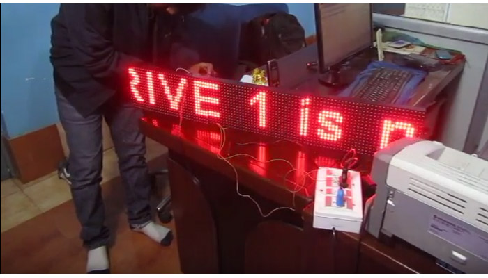
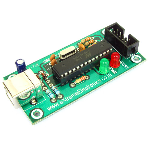
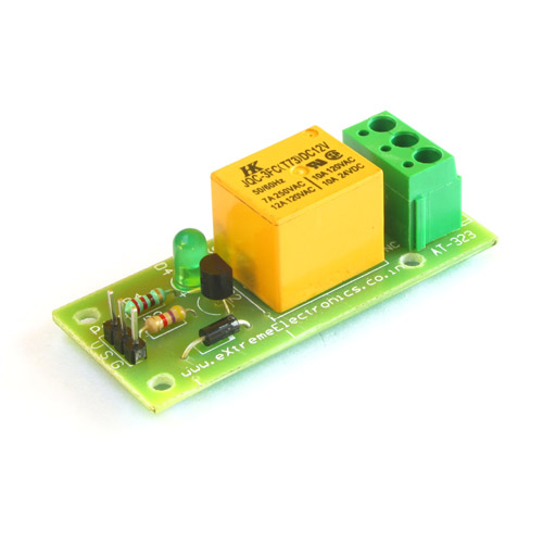
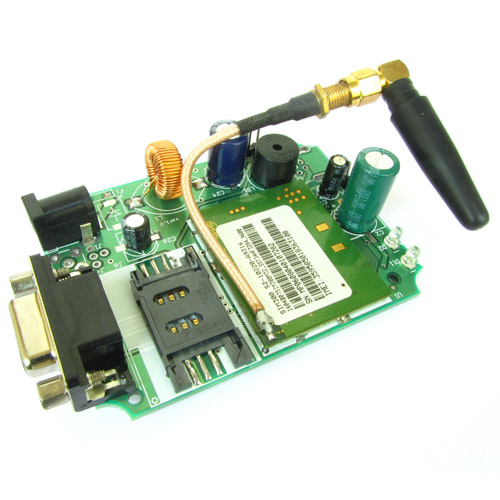
An electronic device is made by using several components like ICs, transistors, diodes, capacitors, resistors, displays, indicators, switches, buttons, connectors etc. All these are connected to other components according to a schematic. A printed circuit board helps hold all components of a device in one place as a single unit and at the same time provide required electrical connection between pins of components.

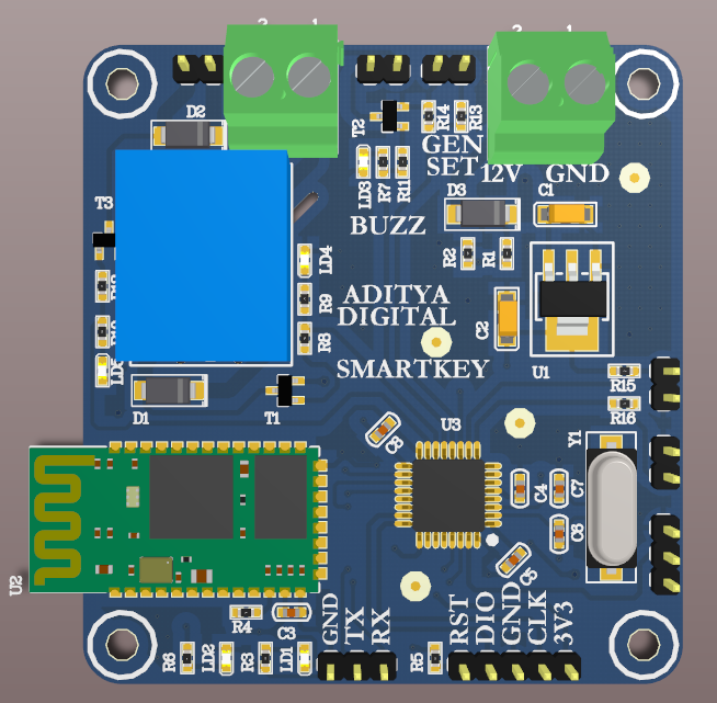
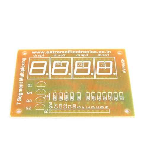
A PCB holding all components together
PCB is about 1.6mm thick rigid piece of flat board. It can be in any two dimensional shape chosen to fit in the enclosure of the device. But mostly they are square, rectangle or sometimes circular in shape.
A PCB has two sides one is called the component side. On this side components are placed. The other side is the solder side. On this side pins of the components are solder to the pads.

Solder side of PCB
Component Side
On the component side, outline of components and their reference numbers are printed. This printing is called the silk screen layer. It helps the user know where and how the components will be placed on the PCB.
For example if a circuit has two resistors they would be referred by names such as R1 and R2 etc. So in this case R1 and R2 would be clearly printed to help you understand which resistor is R1 and which is R2.
Silkscreen layer also helpful in marking others things too so that the user can get some clue about the working of that specific component. For example you can place a text that says "power" next to a LED that indicates power status of the board.
Finally it is also used to show the name of the board, name of the manufacturer or designer, version number of board.

Silkscreen printing on PCB
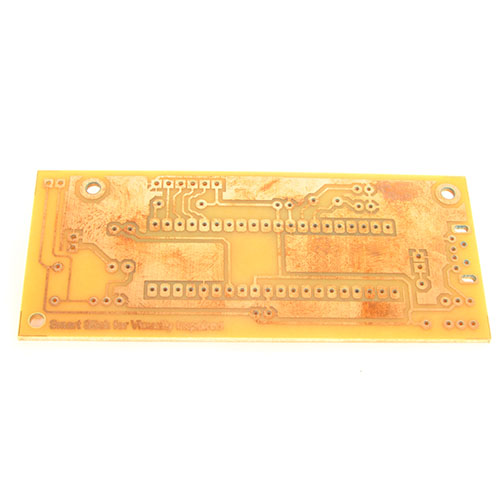
Solder Side
This side has the pads and tracks.
PADS: They are points where the leads of components are soldered to the PCB. They may be circular, square or rectangular in shape. They are made up of conductive copper but covered with a shiny layer of solder so it does not actually looks like copper. This layering is done to increase the ease of soldering. And it also saves the copper for corrosion.
TRACKS: Tracks are used to make electrical connection between pads. They are also made up of copper.
The whole solder side of the PCB is coated with a solder mask which may be green or blue or red in colour. Only the pads are not covered with this as they require soldering. In the PCB shown on this article the solder mask colour is red.
We cordially thanks the following peoples who shared this page on various social networks and insprided us to develop more quality contents!
Zafar, Mulyadi, Hanumant Dhande, Niranjan, Joseph, Pankaj,