Our client Mr. Russel D'Silva needed a device which is capable of
capturing multiple inputs which are on/off, free contact type. That means
it should be able to sense when a contact (relay or contactor) is made.
Several such inputs, say 24 or more were required to be sensed. This data
should be then sent to another display unit which was far away from the
point where inputs where available. According to the inputs the display
would change, the display is a LED dot matrix type and displays scrolling
text messages. The display is about 6 inches in height and about 8 feet
long. The display is clearly visible from a distance of 20 feets.
Our expert engineers designed the product as per Mr. D'Silva's need. We
used a 74HC165 serial in parallel out IC to read input contacts. Input
cards were made in a modular design, each card has one shift register IC
and thus 8 inputs. The design was made in such a way that several such
cards could easily be cascaded to increase number of inputs. Another PCB
was made, which has a ATmega8 MCU and an RS485 interface. The program on
ATmega8 reads the inputs via shift registers and then sends them on RS485
bus. The RS485 is an industry standard communication interface which works
very long range and needs only two wires. Thus inputs from all 24 contacts
needs just two wires to send long way to the display unit.
8
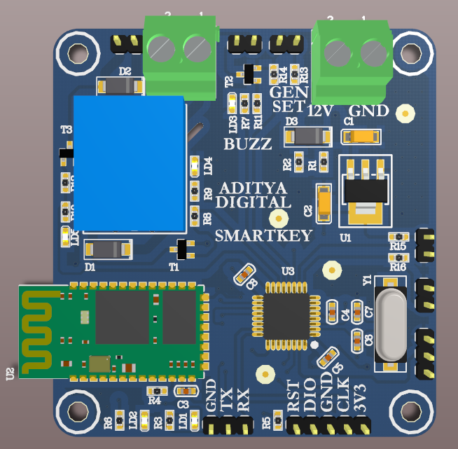
Channel Input Card with IsolationATmega8
with RS485 Interface
PCBs forms the base of any electronic product. With a good quality PCB ready in hand, production becomes very efficient and fast. The product is very durable that is made on a PCB and gives a very professional look also.
We can help to bring to life any PCB design that you may have in your mind for your next project. We have more than 8 years of experience in PCB design thus we can help you easily plan your board by taking required inputs clues from your discussion.
The first step of PCB design is schematic capture. This means drawing a schematic of your hardware using a schematic design CAD PC software. You need to give us a rough circuit diagram drawn by hand on paper so that we can understand your requirement. Other wise you may tell us how your hardware should function and we will draw the circuit diagram ourself.
The next step is creation of board. You should give us exact details about the size and shape requirement of the board if your board need to be of some exact shape or size. Otherwise we may suggest you the optimal shape and size of the board. Another important things that you should clarify if that what type of connectors would be used for various input and output points like power and other things and also their position in the board. A rough hand drawn representation is helpful. After all these things are clear, we would place the components on their optimal location on the board and then route the traces. Routing means inter-connecting the pins of various components.
Schematic Capture
Placement and Routing
Final PCBs
Need our service?
We provide quality and cost effective service to design printed circuit boards as per your requirement